- 您现在的位置:买卖IC网 > Sheet目录1991 > CS5509-ASZR (Cirrus Logic Inc)IC ADC 16BIT SGL SUPP 16-SOIC
CS5509
DS125F3
7
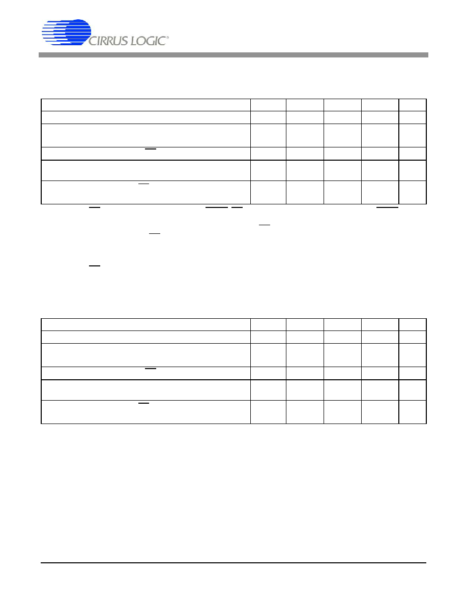
Notes: 16. If CS is activated asynchronously to DRDY, CS will not be recognized if it occurs when DRDY is high
for 2 clock cycles. The propagation delay time may be as great as 2 fclk cycles plus 200 ns. To guarantee
proper clocking of SDATA when using asynchronous CS, SCLK(i) should not be taken high sooner than
2 fclk + 200 ns after CS goes low.
17. SDATA transitions on the falling edge of SCLK. Note that a rising SCLK must occur to enable the serial
port shifting mechanism before falling edges can be recognized.
18. If CS is returned high before all data bits are output, the SDATA output will complete the current data
bit and then go to high impedance.
5V SWITCHING CHARACTERISTICS (T
A = 25 °C; VA+, VD+ = 5V ±5%; Input Levels: Logic 0 =
Parameter
Symbol
Min
Typ
Max
Unit
Serial Clock
fsclk
0-
2.5
MHz
Serial Clock
Pulse Width High
Pulse Width Low
tph
tpl
200
-
ns
Access Time
CS Low to data valid (Note 16)
tcsd
-60
200
ns
Maximum Delay Time
(Note 17)
SCLK falling to new SDATA bit
tdd
-150
310
ns
Output Float Delay
CS High to output Hi-Z (Note 18)
SCLK falling to Hi-Z
tfd1
tfd2
-
60
160
150
300
ns
3.3V SWITCHING CHARACTERISTICS (T
A = 25 °C; VA+ = 5V ±5%; VD+ = 3.3V ±5%; Input
Parameter
Symbol
Min
Typ
Max
Unit
Serial Clock
fsclk
0
-
1.25
MHz
Serial Clock
Pulse Width High
Pulse Width Low
tph
tpl
200
-
ns
Access Time
CS Low to data valid (Note 16)
tcsd
-100
200
ns
Maximum Delay Time
(Note 17)
SCLK falling to new SDATA bit
tdd
-400
600
ns
Output Float Delay
CS High to output Hi-Z (Note 18)
SCLK falling to Hi-Z
tfd1
tfd2
-
70
320
150
500
ns
发布紧急采购,3分钟左右您将得到回复。
相关PDF资料
CS5512-BSZ
IC ADC 20BIT EXTERNAL OSC 8-SOIC
CS5526-BSZR
IC ADC 20BIT W/4BIT LATCH 20SSOP
CS5528-ASZR
IC ADC 24BIT 8CH 24-SSOP
CS5529-ASZR
IC ADC 16BIT W/6BIT LATCH 20SSOP
CS5530-ISZR
IC ADC 24BIT 1CH W/LNA 20-SSOP
CS5534-ASZR
IC ADC 24BIT 4CH W/LNA 24-SSOP
CS5534-BSZR
IC ADC 24BIT 4CH W/LNA 24SSOP
CS5550-ISZR
IC ADC 2CH LOW-COST 24-SSOP
相关代理商/技术参数
CS5510
制造商:CIRRUS 制造商全称:Cirrus Logic 功能描述:16-bit and 20-bit, 8-pin ΔΣ ADCs
CS5510_09
制造商:CIRRUS 制造商全称:Cirrus Logic 功能描述:16-bit and 20-bit, 8-pin ΔΣ ADCs
CS5510-AS
功能描述:模数转换器 - ADC 16-Bit Delta Sigma ADC Ext. OSC RoHS:否 制造商:Texas Instruments 通道数量:2 结构:Sigma-Delta 转换速率:125 SPs to 8 KSPs 分辨率:24 bit 输入类型:Differential 信噪比:107 dB 接口类型:SPI 工作电源电压:1.7 V to 3.6 V, 2.7 V to 5.25 V 最大工作温度:+ 85 C 安装风格:SMD/SMT 封装 / 箱体:VQFN-32
CS5510-ASR
功能描述:模数转换器 - ADC IC 16-Bit 8-Pin Delta Sigma ADC RoHS:否 制造商:Texas Instruments 通道数量:2 结构:Sigma-Delta 转换速率:125 SPs to 8 KSPs 分辨率:24 bit 输入类型:Differential 信噪比:107 dB 接口类型:SPI 工作电源电压:1.7 V to 3.6 V, 2.7 V to 5.25 V 最大工作温度:+ 85 C 安装风格:SMD/SMT 封装 / 箱体:VQFN-32
CS5510-ASZ
功能描述:模数转换器 - ADC 16-Bit Delta Sigma ADC Ext. OSC RoHS:否 制造商:Texas Instruments 通道数量:2 结构:Sigma-Delta 转换速率:125 SPs to 8 KSPs 分辨率:24 bit 输入类型:Differential 信噪比:107 dB 接口类型:SPI 工作电源电压:1.7 V to 3.6 V, 2.7 V to 5.25 V 最大工作温度:+ 85 C 安装风格:SMD/SMT 封装 / 箱体:VQFN-32
CS5510-ASZ
制造商:Cirrus Logic 功能描述:A/D Converter (A-D) IC
CS5510-ASZR
功能描述:模数转换器 - ADC IC 16-Bit 8-Pin Delta Sigma ADC RoHS:否 制造商:Texas Instruments 通道数量:2 结构:Sigma-Delta 转换速率:125 SPs to 8 KSPs 分辨率:24 bit 输入类型:Differential 信噪比:107 dB 接口类型:SPI 工作电源电压:1.7 V to 3.6 V, 2.7 V to 5.25 V 最大工作温度:+ 85 C 安装风格:SMD/SMT 封装 / 箱体:VQFN-32
CS5511
制造商:CIRRUS 制造商全称:Cirrus Logic 功能描述:16-bit and 20-bit, 8-pin ΔΣ ADCs